So, I had some issues with installing the GPU in the case, and the GPU bottom (those metals things at the bottom) ended up scratching part of the motherboard. From what I can tell, there’s a bunch of similar components all the way up, so I’d think there’s redundancy, so I guess it’s not that important. Here is a picture:
https://i.postimg.cc/7LBwkr3h/62e626.jpg
https://files.catbox.moe/62e626.jpg
PC boots fine into bios, fans work, stuff are recognized, mouse and keyboard also works, but I haven’t really done much beyond that.
Motherboard is: MSI B650 Gaming Plus Wifi
It’s located here, and on them, it is written K72 then vertically smaller K2 (the 2 has an underline):
https://i.postimg.cc/XJNcnppT/modelblock-gaming-pd.png
https://files.catbox.moe/7otcn6.png
Should I get a new motherboard?
Edit: Better quality image, and new image host added.


Are those near a connector (maybe on the other side?)Could be a bunch of ESD protection diodes which only come in to play if you wear socks on carpet and touch the connector terminals.Can you provide the numbers listed on the parts? Usually just 3 numbers/letters.Also, looking at the circuit traces, does it look like all three terminals are connected? Is one connected to the ground plane? (The copper that covers most of the board surface around the circuit traces).Edit: looks like they’re 2N7002 MOSFETs
https://www.diodes.com/assets/Datasheets/ds11303.pdf
These act like a digital switch that can use a small voltage to toggle a larger current. Odd to have so many, you normally wouldn’t use a bunch in parallel instead of just a larger FET.
So they look like they’re all connected to the same traces?
From the TI briefing note:
It would also provide redundancy in case of a failure—if you had only one, and it failed (or was scraped off by an over-enthusiastic GPU installation), you would probably not be going to space today.
Can you link that note?
I think that’s usually the method in high power applications where heat dissipation is paramount. Each of these diodes is only rated for 210mA of drain current. From a BOM cost perspective, it’d be much cheaper to just buy one 5A FET rather than parallelizing a bunch of 0.21A FETs. That 5A FET would be in a package that could handle whatever heat it generates.
You’re probably right—I searched for ‘20 mosfets in parallel’ or something like that and it came up near the top. But I didn’t read the whole thing.
I guess there’s got to be some reason for using so many though?
So I guess, what this means is having one scrapped off or failing isn’t a big issue (because of built-in redundancy accounting exactly for that)?
My gut feeling is they didn’t put 20 there in case you scraped one off. But likely the others will have enough leeway to cover for it. If the power rail gets stressed enough, it might well fail sooner than it would have.
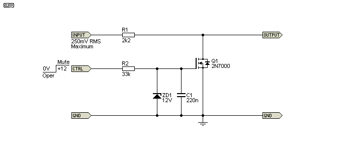
My other running theory is that (due to relative proximity to audio chip), they’re muting FETs for muting audio channels when connecting headphones/speakers to prevent speaker pop.
Interesting. Is the orange line on the board separating the audio section from the rest?
Possibly. Might be marking some isolation or just a stylistic choice by the designer.
It’s like well, here I guess:
https://i.postimg.cc/XJNcnppT/modelblock-gaming-pd.png
You might be able to find a better resolution image of the board if you look, on them, it is written K72 then vertically smaller K2 (the 2 has an underline).
There are so many as you say, so makes me think, there’s enough redundancy to leave it be.
Here’s another idea. In that image, directly below these FETs you can see the little crab logo on the chip. That’s the audio driver. It’s possible these FETs are muting FETS for the analog audio channels. Basically they hold the audio lines down while you connect/disconnect your audio devices to prevent speaker pop.
Like this:
I’ve seen some designs that use two FETs per channel which could explain why there’s so many.
That mb appears to have 8 channel audio on the backplane (7.1) and maybe another stereo header for the front panel headphones? That would make 10 channels in total which fits…